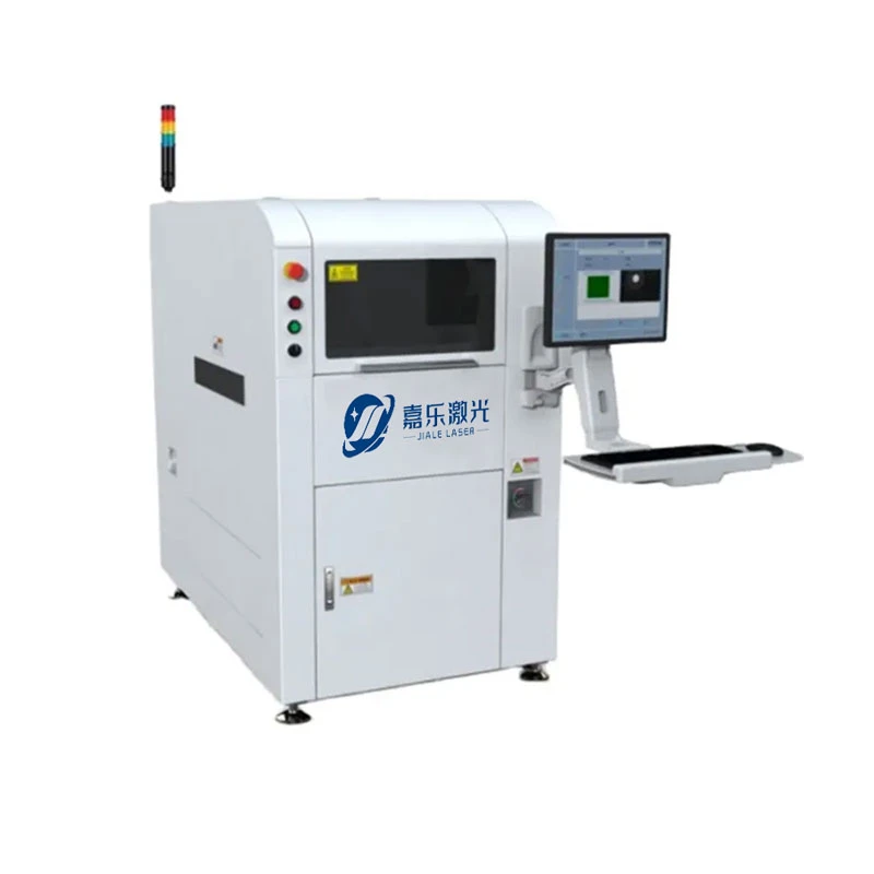
Exploring PCB Laser Cutting Process
As a core component of modern electronic devices, PCBs are widely used in communications, computers, automotive electronics, and consumer electronics. With the rapid miniaturization and integration of electronic devices, higher demands are placed on the design precision and manufacturing processes of PCBs.
Laser cutting technology, due to its advantages such as high precision, high flexibility, and low heat-affected zone, has gradually become an important research direction in the field of PCB cutting.
Table of Contents
PCB Laser Cutting Principle
Precision cutting is achieved by irradiating the PCB surface with a high-energy laser beam (usually a UV laser or a CO2 laser) and instantly vaporizing the material through a photothermal effect.
Cutting Methods
Ablation Cutting: Vaporizes material layer by layer; suitable for complex contours.
Scribble Cutting: Deep grooves are etched into the sheet material, which is then separated mechanically.
Advantages of PCB laser cutting
Ultra-high precision
Knock width: 20–50μm (UV laser), with positioning accuracy up to ±0.01mm.
Suitable for micro-hole and irregular shape cutting of HDI boards (such as the internal structure of earphone compartments).
No mechanical stress
Avoids material delamination or micro-cracks caused by traditional milling cutters, especially suitable for thin plates (<0.2mm) and rigid-flex boards.
Flexibility
Directly imports Gerber files into the software, allowing for quick design switching, suitable for sample prototyping and small-batch, multi-variety production.
Applications of PCB laser cutting
Precision Shape Cutting
PCB for smart wearable devices (e.g., inner board of TWS earphone charging case).
Board Separation Processing
Replacing V-Cut with panel cutting for stamp-hole connections.
Special Structure Processing
Slotting and cutting antenna isolation areas and shielding cover mounting positions.
Frequently Asked Questions
Seam carbonization
Use nitrogen protection and optimize the power/speed ratio.
Copper foil burrs
Add laser trimming paths, or use a secondary precision cutting mode.
Heat-affected zone (HAZ)
UV laser + HIGH-SCAN technology can control HAZ to <15μm.
Conclusion
PCB laser cutting has evolved from an optional process to a standard feature in precision manufacturing. Its core capabilities—non-contact, high precision, high flexibility, and low damage—make it well-suited to the miniaturization, high density, and high reliability trends in electronic products. From principles and light source selection to process control and intelligent upgrades, laser technology continues to break through the boundaries of traditional processing, becoming a key support for the PCB industry’s move towards high-end manufacturing.